Advantages and notes of dual-sided irradiation
Posted date:July 06, 2023Last updated:July 06, 2023
When the material to be irradiated is considerably thicker than the penetration depth, dual-sided irradiation can be used to obtain an effect on the entire material.
Advantages of dual-sided irradiation
When the material to be irradiated is considerably thicker than the penetration depth, the back surface of the material may not be sufficiently irradiated to achieve the desired effect from the electron beam irradiation. In this case, the desired effect can be obtained by irradiating from the back surface of the material as well.
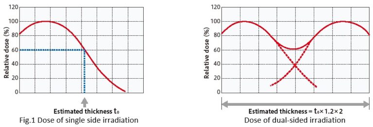
We recommend that the thickness at which the relative dose on the vertical axis of the depth-dose curve reaches 60% (80% in the case of curing) as the thickness that can be processed at that acceleration voltage.
When irradiating thick materials, the relative dose is less than 60% at a depth greater than a certain thickness, resulting in areas where the irradiation effect is not sufficient. In this case, the irradiation effect can be obtained over the entire area by re-irradiating from the back side of the material. In dual-sided irradiation, the dose from the front surface overlaps with the dose from the back surface, so thatirradiation effects can be achieved up to 2.4 times the thickness of materials irradiated on one side, as shown in Figure 1.
Irradiation to provide gradient function
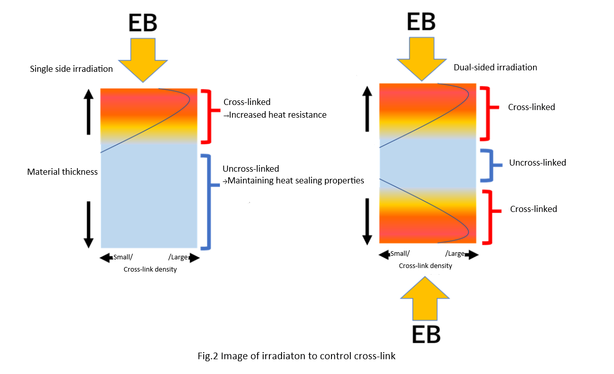
By selecting the energy of the electron beam relative to the thickness of the irradiated material, the crosslink density in the direction of material thickness can be controlled.
In single side irradiation, the irradiated surface is given functions such as heat resistance, while the non-irradiated surface is left with heat sealing properties. (Figure 2 left).
In dual-sided irradiation, the difference in crosslink density between the surface and the interior canbe used to control foam size, etc. (Figure 2 right)
Notes of dual-sided irradiation
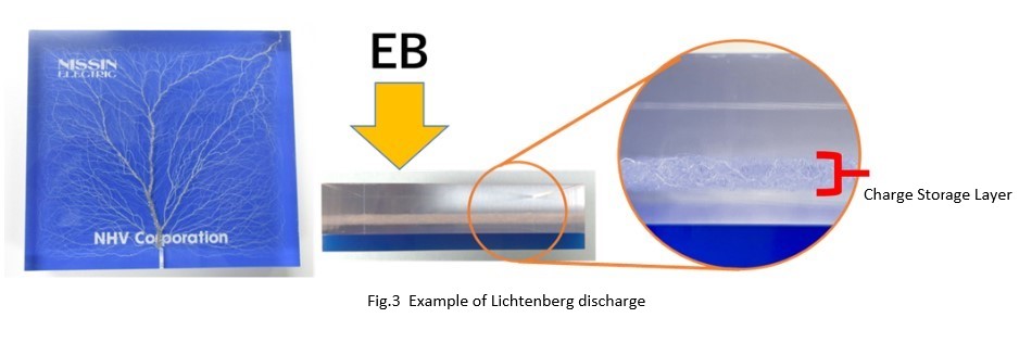
Irradiated electrons accumulate at the penetration depth. This accumulation is called “charge-up”.
The accumulated electrons move from the inside to the surface of the irradiated material by some trigger, and an electrical discharge phenomenon occurs (this is called Lichtenberg discharge).
This discharge leaves dendritic discharge traces in the area where the electrons have moved, and the irradiated material becomes defective.
This charge-up is less likely to occur when the volume resistivity is around 1E11 to 1E15 Ω-cm, since electrons move little by little as needed, but it is more likely to occur when the volume resistivity is 1E16 Ω-cm or higher.
If the volume resistivity is greater than 1E16 Ω-cm, the above discharge can be avoided by increasing the penetration depth greater than the thickness of the material.
Since it is also related to dose and dose rate, verification by test irradiation and sufficient consideration are necessary to determine the production conditions.
Figure 3 shows an example of irradiating PMMA and intentionally generating and discharging “charge-up”.
Summary
When treating thicker materials, irradiating from both the front and the back is more effective because irradiation from only a single side leaves the back side untreated.
Therefore, dual-sided irradiation, in which irradiation is performed from both the front and back surfaces, is the most effective means to achieve the desired results for your material.
Since the dose of electron beams varies as they enter the material, their effect on the thickness direction of the irradiated material is not constant. This can be considered a disadvantage of electron beam irradiation, but it is sometimes used to produce different effects on the surface and back surface.
It is important to select the appropriate acceleration voltage and irradiation method according to the desired effect.
[Inquiry]
NHV Corporation
Please inquire through the inquiry form.